Fixing the CH341A Programmer's Stuck-at-5V Dataline Bug
Most cheap CH341A EEPROM programmers, the black boards with the gold edge, carry a hardware bug in versions before 1.7. Jumper the board to 3.3V, and the data lines still sit at 5V. Flash a 3.3V chip, like the ones in most Thingino cameras, and that stray 5V reaches pins the chip was never rated for.
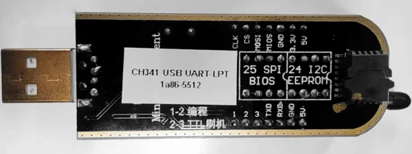
This fix is not original work. It was worked out by @ddemos1963 and first written up on the thingino-firmware wiki’s CH341A Programmer page. This post covers that fix on its own, with the same photos, so it stands alone. Full credit stays with the original page and its author.
The circuit
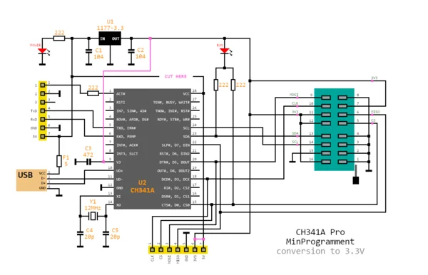
The schematic below shows the whole conversion. A 3.3V regulator, U1, an AMS1117-3.3, already sits on the board. The point marked CUT HERE is where the stock design ties pin 9 (V3) of the CH341A to the unregulated 5V rail, instead of to that regulator’s output.
The fix (boards before v1.7)
- Flip the board over. Cut the trace connecting the 5V power line to the CH341A chip, using a sharp utility knife.
- Bridge the 3.3V output leg of the onboard regulator to pin 9 of the CH341A IC. Use the corresponding trace at the nearby capacitor, labeled
C3. - Re-route power to the chip: connect the 3V3 pin to pin 28 of the CH341A IC through the 5V pin on the header.
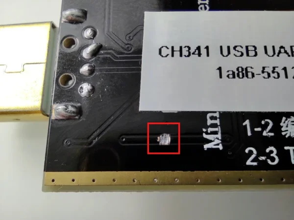
Step 1: the cut trace, on the back of the board.
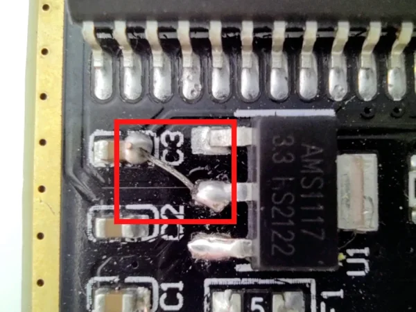
Step 2: the bridge from the regulator’s 3.3V output to pin 9, soldered across the C3 pads.
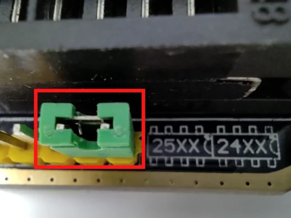
Step 3: power restored to the rest of the board through the header’s 5V pin, now carrying 3.3V.
That is the whole mechanical change: cut one 5V path, feed pin 9 and pin 28 from the 3.3V regulator instead.
Newer boards (V1612, sold on Amazon US, confirmed August 2025)
Some recent V1612 units route their traces differently, and the capacitor labeled C3 on the original boards is C4 here. The three-step logic is identical. Only the exact physical work changes.
Preventing the clip from back-feeding the camera
The fix above solves the 5V dataline bug. A second, separate risk shows up only when the clip is used in-circuit, on a camera board that still has its own power connected.
The clip carries all eight ZIF socket pins straight to the target chip, including pin 8, VCC. Cheap camera boards carry no diode, and no other protection, between that chip’s VCC pin and the rest of the board’s power rail. With pin 8 connected, the programmer’s own 3.3V supply feeds straight into the camera board through that same rail.
The camera then draws its normal operating current from that rail. The programmer is now the thing supplying that current. It comes out of the programmer’s small onboard regulator, not the camera’s own power source. That regulator was never sized for a whole camera board’s load. It overcurrents, and the circuit browns out.
The fix: keep pin 8 from ever reaching the chip. A small piece of tape over that one ZIF socket contact on the clip is enough.
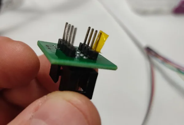
The chip still gets power once pin 8 is disconnected, but not through a dedicated supply pin. It draws that power parasitically, mostly through the ESD protection on the remaining data and clock lines. That is usually enough, because the chip’s own current draw normally sits below what those pins can supply this way. It is not a guaranteed fix. A chip that draws more current than usual, or a board where that parasitic path is weaker, can still leave taping pin 8 alone unable to complete a read or write.
If taping pin 8 does not get a working session, there is a second option. It is a last resort: power the camera normally, and short pins 5 and 6 on the flash chip while it boots. Powering the camera this way gives the chip proper current from the board’s own supply. That replaces the weaker parasitic path the tape fix relies on. The short itself drops the SoC into its bootloader mode. In that mode, the SoC does not issue SPI reads or writes to the flash chip on its own. It waits for further commands first. With the SoC not driving the SPI lines, there is no contention between the SoC and the external programmer for those same lines. Interrupting the normal boot this way lets the programmer write to the chip while the board runs on its own power. A short jumper wire, a screwdriver tip, or tweezers held across pins 5 and 6 for the first few seconds of boot is enough. Once the SoC has latched into bootloader mode and the programmer detects the chip, the short can be released. Try the tape fix first. Reach for this procedure only when that fix does not work.
What you learned
- Boards before v1.7 hold their data lines at 5V even when jumpered to 3.3V. Cut the 5V trace to the CH341A chip, bridge 3.3V to pin 9, and feed the rest of the board through pin 28.
- V1612 boards route differently. Bridge from capacitor
C4instead ofC3. The rest of the fix is identical. - In-circuit clip use on a live camera board can back-feed the board through the clip’s pin 8, since these boards carry no protection against it. Tape over that one ZIF socket contact to stop it.
- The chip still gets power once pin 8 is taped, through parasitic current on the remaining pins. That is not always enough to complete a read or write.
- When it is not enough, power the camera normally and short pins 5 and 6 on the flash chip for the first few seconds of boot. That drops the SoC into bootloader mode, where it does not drive the SPI lines on its own, and the short can be released once the programmer detects the chip.
Sources
- Original write-up and full photo set: thingino-firmware wiki, CH341A Programmer
- Fix credited to @ddemos1963
- DIY BCQ CH341A forum thread (Chinese, use Chrome’s automatic translation)
- 4PDA CH341A Programmer thread (Russian, use Chrome’s automatic translation)